AR
C
HIVE INF
O
RMATI
O
N
ARCHIVE INFORMATION
MRF6S9045NR1 MRF6S9045NBR1
3
RF Device Data
Freescale Semiconductor
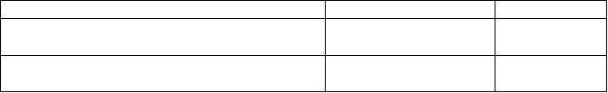
Table 5. Electrical Characteristics (TC
= 25
°C unless otherwise noted)
(continued)
Characteristic
Symbol
Min
Typ
Max
Unit
Typical GSM EDGE Performances
(In Freescale GSM EDGE Test Fixture Optimized for 921-960 MHz, 50 ohm system)
VDD
= 28 Vdc, IDQ
= 350 mA, Pout
= 16 W Avg., f = 921-960 MHz, GSM EDGE Signal
Power Gain
Gps
?
20
?
dB
Drain Efficiency
ηD
?
46
?
%
Error Vector Magnitude
EVM
?
1.5
?
%
Spectral Regrowth at 400 kHz Offset
SR1
?
-62
?
dBc
Spectral Regrowth at 600 kHz Offset
SR2
?
-78
?
dBc
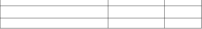
Typical CW Performances
(In Freescale GSM Test Fixture Optimized for 921-960 MHz, 50 ohm system) V
DD
= 28 Vdc,
IDQ
= 350 mA, Pout
= 45 W, f = 921-960 MHz
Power Gain
Gps
?
20
?
dB
Drain Efficiency
ηD
?
68
?
%
Input Return Loss
IRL
?
-12
?
dB
Pout
@ 1 dB Compression Point
(f = 940 MHz)
P1dB
?
52
?
W


发布紧急采购,3分钟左右您将得到回复。
相关PDF资料
MRF6S9060NR1
MOSFET RF N-CH 28V 14W TO-270-2
MRF6S9125MR1
MOSFET RF N-CH 28V 27W TO-270-4
MRF6S9125NR1
MOSFET RF N-CH 28V 27W TO-270-4
MRF6S9130HSR5
MOSFET RF N-CHAN 28V 27W NI-780S
MRF6S9160HSR5
MOSFET RF N-CHAN 28V 35W NI-780S
MRF6V10010NR4
MOSFET RF N-CHAN PLD-1.5
MRF6V10250HSR5
MOSFET RF N-CH NI780S
MRF6V12500HR5
FET RF N-CH 1.03GHZ 100V NI-780H
相关代理商/技术参数
MRF6S9045NR1_08
制造商:FREESCALE 制造商全称:Freescale Semiconductor, Inc 功能描述:RF Power Field Effect Transistors N-Channel Enhancement-Mode Lateral MOSFETs
MRF6S9060
制造商:FREESCALE 制造商全称:Freescale Semiconductor, Inc 功能描述:RF Power Field Effect Transistors
MRF6S9060MBR1
功能描述:MOSFET RF N-CH 28V 14W TO-272-2 RoHS:否 类别:分离式半导体产品 >> RF FET 系列:- 产品目录绘图:MOSFET SOT-23-3 Pkg 标准包装:3,000 系列:- 晶体管类型:N 通道 JFET 频率:- 增益:- 电压 - 测试:- 额定电流:30mA 噪音数据:- 电流 - 测试:- 功率 - 输出:- 电压 - 额定:25V 封装/外壳:TO-236-3,SC-59,SOT-23-3 供应商设备封装:SOT-23-3(TO-236) 包装:带卷 (TR) 产品目录页面:1558 (CN2011-ZH PDF) 其它名称:MMBFJ309LT1GOSMMBFJ309LT1GOS-NDMMBFJ309LT1GOSTR
MRF6S9060MR1
功能描述:MOSFET RF N-CH 28V 14W TO-270-2 RoHS:否 类别:分离式半导体产品 >> RF FET 系列:- 产品目录绘图:MOSFET SOT-23-3 Pkg 标准包装:3,000 系列:- 晶体管类型:N 通道 JFET 频率:- 增益:- 电压 - 测试:- 额定电流:30mA 噪音数据:- 电流 - 测试:- 功率 - 输出:- 电压 - 额定:25V 封装/外壳:TO-236-3,SC-59,SOT-23-3 供应商设备封装:SOT-23-3(TO-236) 包装:带卷 (TR) 产品目录页面:1558 (CN2011-ZH PDF) 其它名称:MMBFJ309LT1GOSMMBFJ309LT1GOS-NDMMBFJ309LT1GOSTR
MRF6S9060N
制造商:Freescale Semiconductor 功能描述:MRF6S9060N - Bulk
MRF6S9060NBR1
功能描述:MOSFET RF N-CH 28V 14W TO-272-2 RoHS:是 类别:分离式半导体产品 >> RF FET 系列:- 产品目录绘图:MOSFET SOT-23-3 Pkg 标准包装:3,000 系列:- 晶体管类型:N 通道 JFET 频率:- 增益:- 电压 - 测试:- 额定电流:30mA 噪音数据:- 电流 - 测试:- 功率 - 输出:- 电压 - 额定:25V 封装/外壳:TO-236-3,SC-59,SOT-23-3 供应商设备封装:SOT-23-3(TO-236) 包装:带卷 (TR) 产品目录页面:1558 (CN2011-ZH PDF) 其它名称:MMBFJ309LT1GOSMMBFJ309LT1GOS-NDMMBFJ309LT1GOSTR
MRF6S9060NR1
功能描述:MOSFET RF N-CH 28V 14W TO-270-2 RoHS:是 类别:分离式半导体产品 >> RF FET 系列:- 产品目录绘图:MOSFET SOT-23-3 Pkg 标准包装:3,000 系列:- 晶体管类型:N 通道 JFET 频率:- 增益:- 电压 - 测试:- 额定电流:30mA 噪音数据:- 电流 - 测试:- 功率 - 输出:- 电压 - 额定:25V 封装/外壳:TO-236-3,SC-59,SOT-23-3 供应商设备封装:SOT-23-3(TO-236) 包装:带卷 (TR) 产品目录页面:1558 (CN2011-ZH PDF) 其它名称:MMBFJ309LT1GOSMMBFJ309LT1GOS-NDMMBFJ309LT1GOSTR
MRF6S9125
制造商:FREESCALE 制造商全称:Freescale Semiconductor, Inc 功能描述:RF Power Field Effect Transistors